

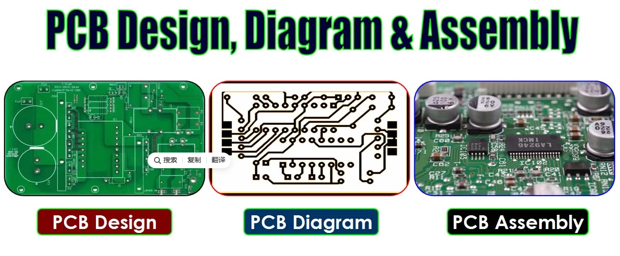
Printed Circuit Board – Design, Diagram and Assembly
Printed Circuit Boards (PCBs) are the heart of all modern electronics – from smartphones and smartwatches to industrial automation and aerospace systems. Whether you are a professional, beginner or an electronics hobbyist, understanding PCB design, diagrams, and assembly is key to building reliable electronic devices.
In this guide, you will learn:
PCB design refers to the process of planning and creating the layout of a printed circuit board (PCB) that connects electronic components using conductive pathways.
PCB assembly (PCBA) involves mounting those components onto the board using THT, SMT or Mixed Technology to create a functional circuit.
The combination of design and assembly is known as Printed Circuit Assembly (PCA), which is the finished product ready for testing and use.
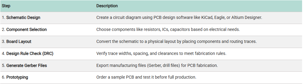
Here are 6 simple steps to design your own PCB:
Check:
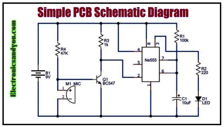
A simple PCB schematic diagram shows how electronic components like resistors, capacitors, diodes, and Integrated Circuits (ICs) are connected. Here is a beginner-friendly example:
This simple design lights an LED using basic electronic components. You can create and visualize such diagrams using free PCB design software like:
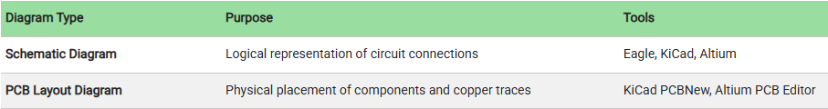
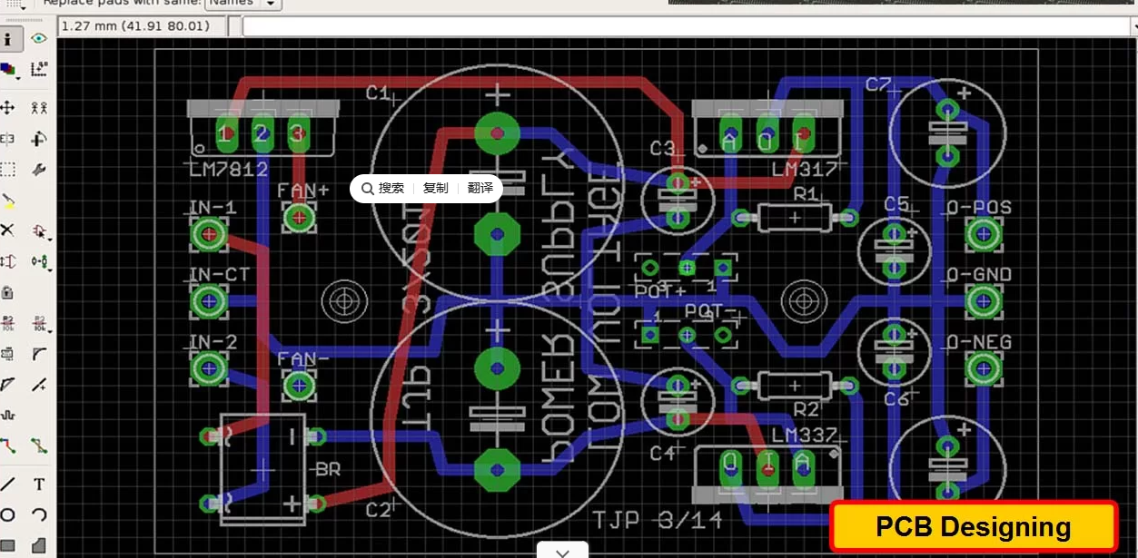
Both diagrams are essential: the schematic helps with understanding the circuit logic, and the PCB Layout focuses on physical connectivity and real-world manufacturability.
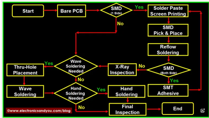
PCB assembly (PCBA) is the process of soldering or mounting components onto a manufactured bare PCB. Here are the basic steps involved in SMT PCB Assembly Process:
Suppose you are designing a smart thermostat. You would use PCB design software to:
This workflow applies across IoT devices, consumer electronics, and medical instrumentation.
